This distributed ICTS consists of four infrastructures:
National Center for Electron Microscopy of Madrid
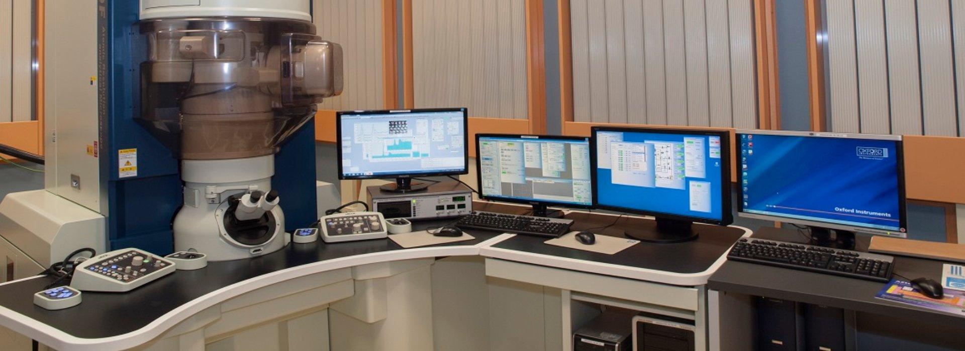
It includes a wide range of transmission, scanning, microwaves, force microscopy equipment and is equipped with state-of-the-art microscopes equipped with aberration correctors. It is worth mentioning the existence of two microscopes with the most advanced technology of the moment and that give uniqueness to the center: an ARM 200cFEG microscope corrected in probe and equipped with state-of-the-art analytical techniques, and a second ARM300cFEG equipment corrected in image (resolution 0.05 nm). These two instruments are complemented by advanced SEM microscopes, as well as a set of SEM/TEM equipment (Transmission Electron Microscopy) that allow to address a complete characterization both at structural and compositional level for a study prior to sub-Angstrom characterization.
Laboratory of Advanced Microscopy of Zaragoza
Its objective is to provide the scientific and industrial communities with the most advanced equipment in local probe microscopes and electronic microscopes for the observation, characterization, nanofabrication and manipulation of materials on the atomic and molecular scale. In addition, it has other laboratories of crucial importance for the characterization, processing and manipulation on the nanometric scale, including a white room (photolithography), double beam techniques for the preparation of samples and other characterization methods based on photoelectronic spectroscopy.
Electronic Microscopy Division of the University of Cadiz
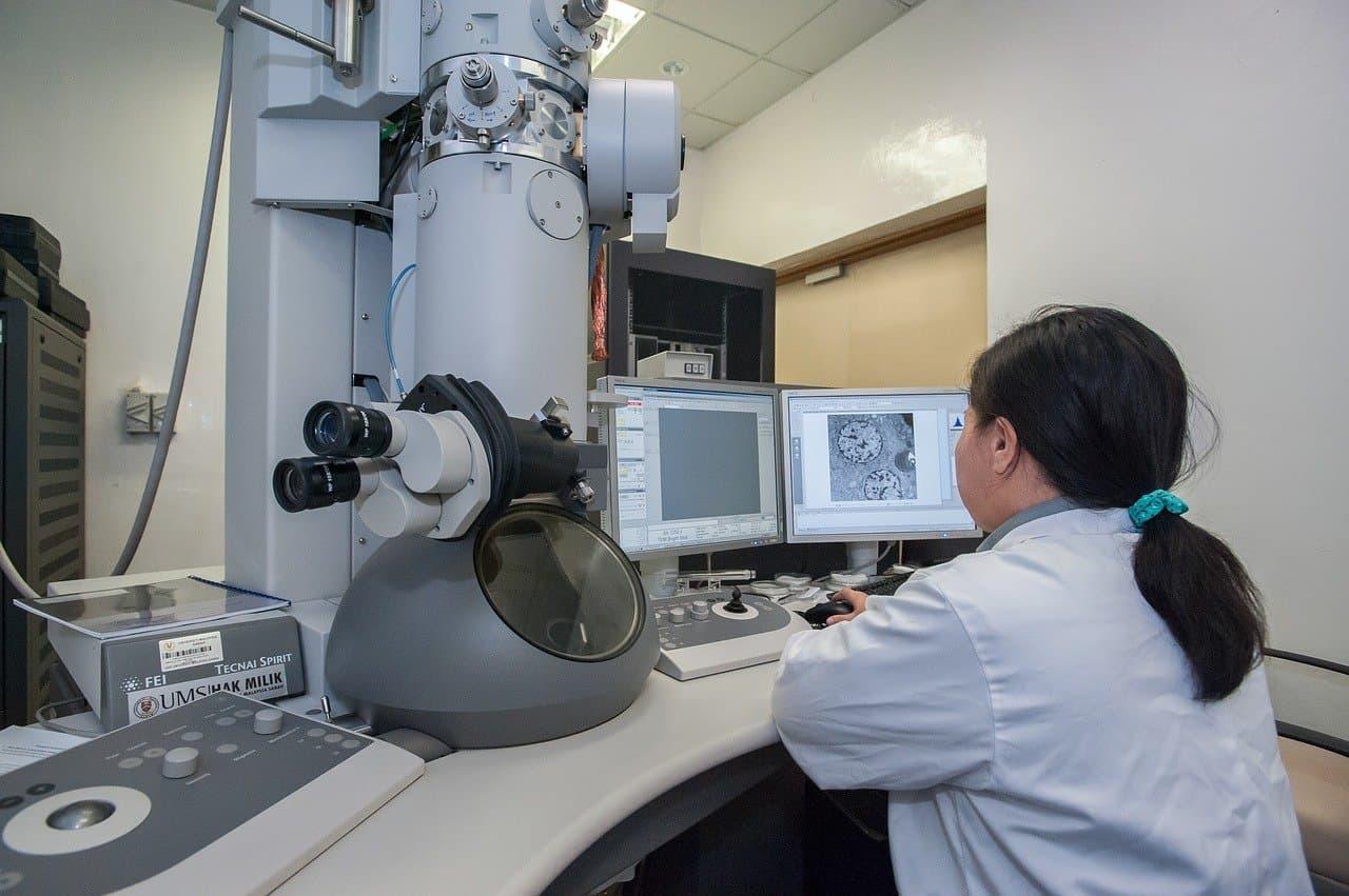
It offers a large battery of microscopy equipment and state-of-the-art support techniques, including the FEIS Titan Themis 60-300 Ultra High Resolution Microscope. This microscope is the only one in Spain doubly corrected, in probe and objective, which allows simultaneous analytical and structural studies to be carried out on the same sample with better resolutions than the Angstrom.
Applied Electron Microscopy of Materials Unit of the University of Barcelona
It has electronic cryomicroscopy equipment for the characterization of materials “sensitive” to the beam, as in the case of biological samples, electrical measurements in situ for the structural characterization by electronic precession and analysis by microprobe for the characterization of minerals of complex composition, as well as STEM microscopy.
As a whole, advanced methods and techniques are offered in transmission and scanning electron microscopy for the structural analysis of materials, sample preparation and treatment of images and data by computational methods, which allow us to address the characterization of complex materials, both inorganic and organic with application in biomedicine, catalysis, intelligent materials, transport, energy and communications.
