This distributed ICTS consists of three infrastructures:
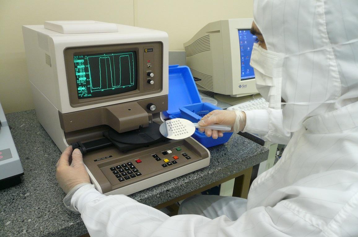
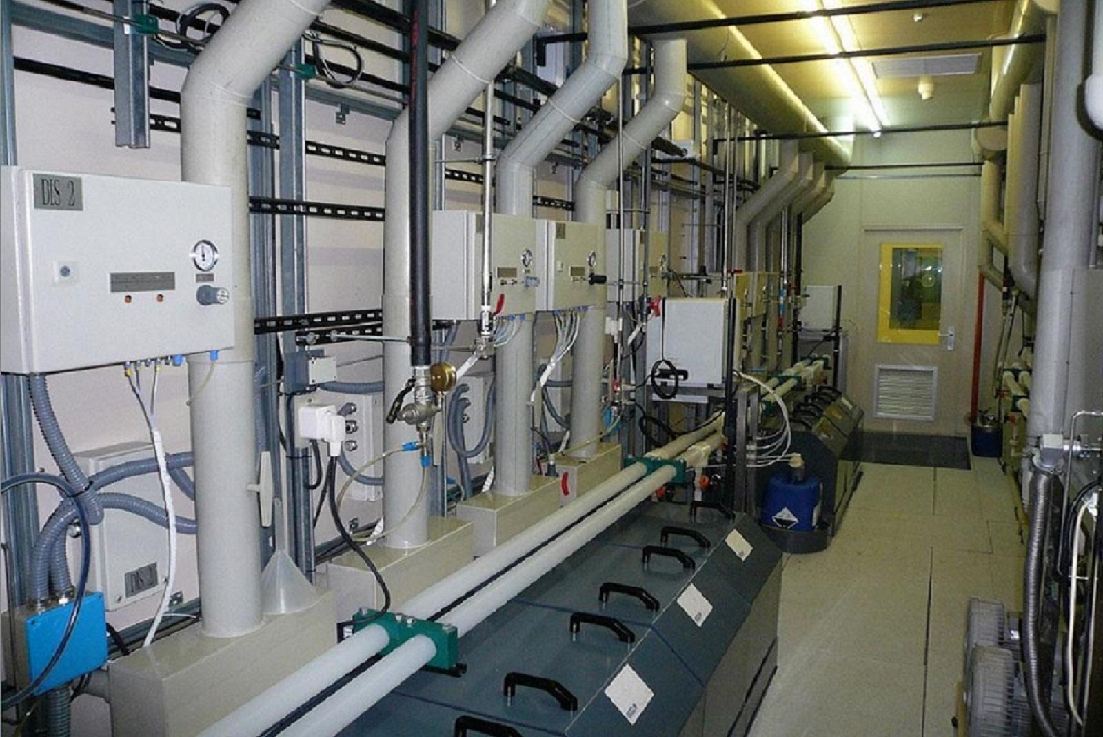
This installation has a complete line of micro-nano manufacturing devices integrated on silicon wafers (150 mm), located in a clean room of 500 m2 that includes the following technological capabilities: optical lithography (mask aligners and steppers) and direct writing by electron gun, deposition of resins and developer, deposition of dielectrics and metals, chemical attacks (wet and dry), ionic implanter, etc. There is also a complete laboratory for the assembly and encapsulation of integrated photonic components, physical and optical characterization laboratories for devices, as well as a laboratory for the characterization of optical systems and networks.
The equipment and advanced instrumentation of this installation allow the manufacture of electronic materials other than silicon, its technological processing and the obtaining of integrated devices and structures of electronic, optical, optoelectronic and magnetic type. Thanks to its electron beam lithography system, it is possible to make structures of micrometric and nanometric size. The facilities consist of 400 m2 of clean rooms, 300 m2 of characterization laboratories and 200 m2 of instrumentation and electronics laboratories.
The range of applications that can be covered in this facility is very wide, including biomedical, environmental, food, energy and mobility, security, communications and consumer electronics, etc. For these applications the main implementations they offer are semiconductor devices including power devices and radiation detectors, sensors, actuators and MEMS (Microelectromechanical Systems), nano-scale devices and actuators and Lab-on-a-Chip systems and polymeric devices.